SprintPCB
Provide the most competitive
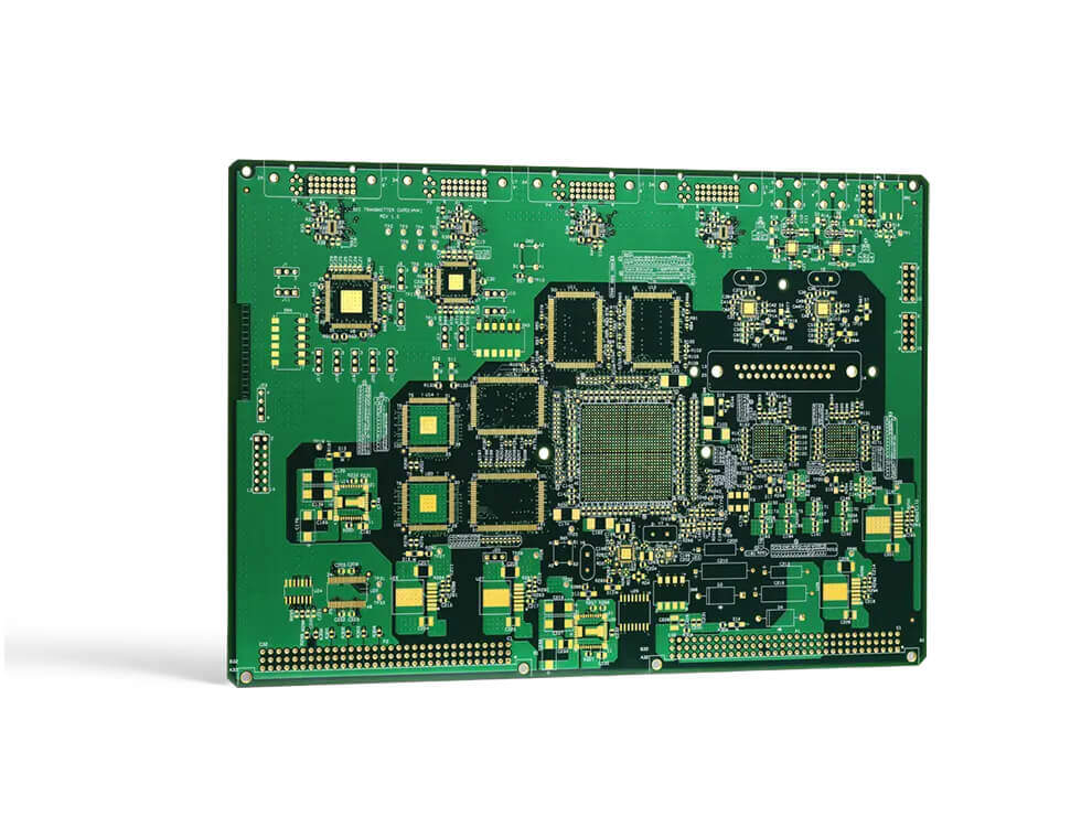
Any layer HDI PCBs

You may be surprised how competitive the right HDI layout can be.
HDI PCB costs can be reduced when your stack-up is properly planned out. Additionally, design efficiencies in HDI production mean faster time-to-market. And in terms of reliability, microvias out-perform typical through-holes almost every time.
Feature | Technical specification |
|---|---|
Number of layers | 4 – 16 layers standard, 22 layers advanced |
Technology highlights | 3+N+3, 4+N+4, any layer |
Materials | FR4 high performance, Dongguan Shengyi |
Copper weights (finished) | 18μm – 70μm |
Minimum line and space | 0.05mm / 0.05mm |
PCB thickness | 0.40mm – 3.20mm |
Surface finishes available | OSP, ENIG, Immersion tin, Immersion silver, Electrolytic gold, Gold fingers |
Why SprintPCB can Provide the most
competitive PCBs
Under the long-term strategic cooperation agreement with laminate supplier , the price we get is 10% cheaper than most competitors
PCB Inner /outer layers fab with LDI equipments, the automotic production reduce our labor cost 5%
Lean manufacturing increases product yield

About SprintPCB
We can provide competitive price and guarantee the
quality requirements of customers without excess
quality. Our technical level can meet most of the
industrial control and consumer products.
2007
Since 2007
39
Markets
2680
Global customers
>95%
On time delivery
Manufacturing Equipment at SprintPCB
SprintPCB operate with most advance equipment in the industry to provide efficient production and high quality products with value added to our partners


Trusted by innovators since 2007
In the race to build tomorrow, SprintPCB engineers and PCB designers continually patent new technologies,
crossing design barriers—to help innovators bring new products to market.
SIEMENS
"I am extremely satisfied with the quality of the PCBs you manufacture. The solder pads on each board are very smooth and the connections are very strong. I have worked with other manufacturers before, but the quality was always subpar. Since switching to SprintPCB, the quality of my projects has significantly improved. Thank you for your outstanding manufacturing process!"
- John Smith

Get High-Quality PCBs at a Fraction of the Cost
Why Pay More for PCB Manufacturing?
Partner with Us for the Best Prices!
FAQs
IPC-2226 defines HDI as a printed circuit board with a higher wiring density per unit area than conventional printed circuit boards (PCB). They have finer lines and spaces ≤ 100 µm / 0.10 mm, smaller vias (<150 µm) and capture pads <400 µm / 0.40 mm, and higher connection pad density (>20 pads/cm2) than employed in conventional PCB technology.
At some level of circuit complexity, turning to an architecture with blind and buried vias will result in better yield and lower cost than would a through-hole design.
HDI PCBs help reduce costs by decreasing size, minimizing the number of components, reducing signal interference, and automating the manufacturing process.
Materials play a large role in terms of manufacturability and direct cost of your circuit board. Here is a tip: The goal is always to select the right material for manufacturability that, at the same time, meets your temperature, and your electrical requirements. When it comes to materials, make sure that your high-speed material is also suitable for your HDI design. They are many other factors that come into play when selecting the proper materials for your design. View more.
It is very safe to assume it is +/- 1 mil accuracy. Usually, in a staggered microvia formation, the diameters of both operate and lower microvias are the same. The key parameter that decides whether the staggering is possible or not, without the lower microvia needing to be filled, is the dimension E, the vertical separation between the central access of the two microvias. For staggering to be viable, the value of E must be greater than the microvia diameter.
CONTACT US
We would love to respond to your queries and help you succeed.
During our business Hours: 9:00~18:00