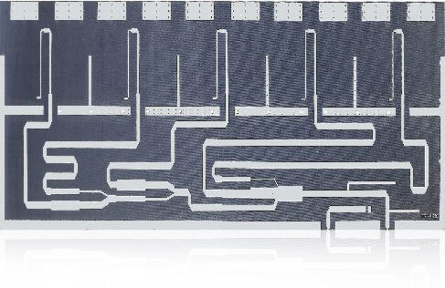
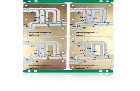
RF – Radio frequency PCBs
Radio frequency (RF) and microwave (MW) circuits can be found in wireless products from handheld devices for medical and industrial applications to advanced communications systems for base stations, radar and global positioning.


When producing radio frequency PCBs, it is important to think about how to control the signals using (i) materials types and material characteristics (loss tangent / Df and dielectric constant / Dk) (ii) low profile copper foils (iii) weave styles and (iv) how we layout the copper circuitry.
Feature | Technical specification |
|---|---|
Number of layers | 2-20 layers |
Technology highlights | Controlled impedance, low loss materials, miniaturization |
Materials | Low loss / low Dk, higher performance FR-4, PPO, Teflon, hydrocarbon / ceramic filled |
Copper weights (finished) | 0.5 OZ – 6 OZ |
Minimum track and gap | 0.075 mm / 0.075 mm |
Metal core thickness | 0.4-2mm post bonded |
Maxmimum dimensions | 580 mm x 650 mm |
Surface finishes available | HASL (Lead-free), OSP, ENIG, Immersion tin, Immersion silver |
Dielectric thickness | 0.1mm – 3.0mm |
Why SprintPCB can Provide the most
competitive PCBs
Under the long-term strategic cooperation agreement with laminate supplier , the price we get is 10% cheaper than most competitors
PCB Inner / outer layers fab with LDI equipment, the automatic production reduce our labor cost 5%
Lean manufacturing increases product yield
About SprintPCB
We can provide competitive prices and guarantee the quality requirements of customers without excess quality. Our technical level can meet most of the industrial control and consumer products.
Trusted by innovators since 2007
In the race to build tomorrow, SprintPCB engineers and PCB designers continually patent new technologies,
crossing design barriers—to help innovators bring new products to market.
"I am extremely satisfied with the quality of the PCBs you manufacture. The solder pads on each board are very smooth and the connections are very strong. I have worked with other manufacturers before, but the quality was always subpar. Since switching to SprintPCB, the quality of my projects has significantly improved. Thank you for your outstanding manufacturing process!"
- John Smith

Get High-Quality PCBs or PCBA at a Fraction of the Cost
Why Pay More for PCB Manufacturing?
Partner with Us for the Best Prices!
FAQ about Radio frequency PCBs
A Radio Frequency (RF) PCB is a type of printed circuit board designed specifically for high-frequency applications in the RF and microwave frequency range, typically ranging from 3 MHz to 100 GHz.
RF PCBs have specific design requirements and construction techniques that differ from regular PCBs. They are designed to handle high-frequency signals with minimal signal loss and interference, and are manufactured with materials that are specially chosen for their electrical and thermal properties.
The materials used in the manufacturing of RF PCBs include specialized high-frequency laminates, copper cladding, and substrate materials. The selection of materials is based on their dielectric constant, loss tangent, and thermal conductivity.
RF PCBs are tested using specialized equipment such as network analyzers, spectrum analyzers, and time-domain reflectometers to ensure their electrical performance meets the specifications required for their intended use.
RF PCBs are commonly used in wireless communication devices such as cell phones, Wi-Fi routers, and satellite communication systems, as well as in medical and military equipment, navigation systems, and scientific instruments.
CONTACT US
We would love to respond to your queries and help you succeed.
During our business Hours: 9:00~18:00
